Scalable disordered architectures on semiconductors of IV group obtained by solid state dewetting
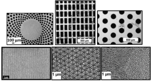
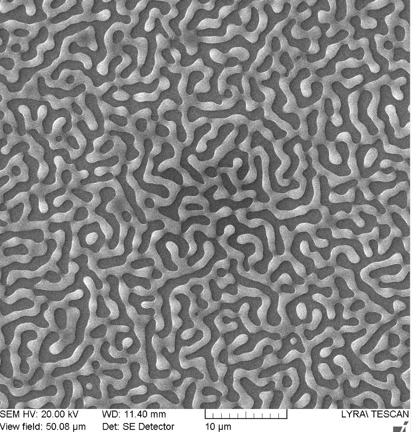
Silicon-based nanocrystals represent a promising resource both for next generation electronic devices and for nano-photonics applications. Their exploitation, however, requires precise size, shape and position control. Owing to their large surface-area-to-volume ratio, thin semiconductor solid films are often unstable upon annealing. As such, under the action of surface diffusion, the film breaks eventually forming isolated islands when heated at temperature well-below the melting temperature of the bulk material. This phenomenon, known as solid-state dewetting (SSD), is one of the main factors impeding the use of ultra-thin silicon films on insulators for the further miniaturization of electronic components.
IFN has demonstrated the ultimate control of Si and SiGe-based thin films dewetting for the precise formation of complex nano-architectures, and their exploitation as dielectric nano-antennas and field-effect transistors wire. SSD indeed is a natural shape instability occurring in thin solid films when heated at high temperature: it transforms a flat layer in isolated islands in a timeframe independent from the sample size.
However, its potential for applications based on complex pattern formation is still unexplored in spite of the manifold advantages it offers: a) it forms monocrystalline and facetted (atomically smooth) structures (size from ~nm up to ~10 µm), free from defects and from the typical roughness produced by conventional etching methods; b) the islands are directly formed on an insulating substrate (SiO2); c) spontaneous dewetting can produce over arbitrary scales patterns that cannot be designed numerically. Therefore, SSD can be efficiently exploited in all these fields to form perfectly ordered and complex nano-architectures over large scales, as well as randomly organized, isolated islands.

Nonlinear photonics with metal-less nanoantennas and metasurfaces
Dielectric metasurfaces and photonic crystals sustain electromagnetic modes which can be exploited to enhance nonlinear frequency-conversion processes such as second or third harmonic generations. IFN employs electron-beam lithography and reactive ion etching to fabricate silicon metasurfaces supporting electromagnetic resonances with different quality factors, ruled by the geometry. This allows to investigate the trade-off between resonant enhancement and matching the spectral bandwidth of the ultrafast excitation source.